Olympus
scope2
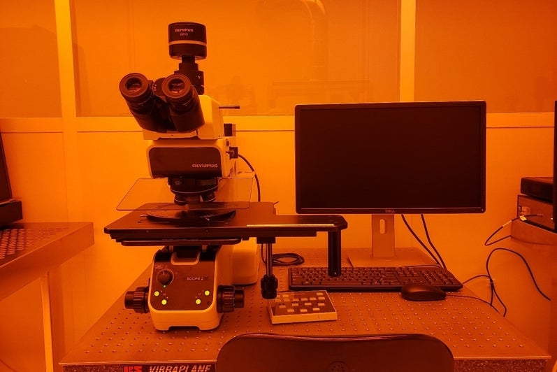
What it is
General reference — not yet source-verifiedThe Olympus scope2 is a semiconductor inspection microscope used for the visual examination and documentation of wafers, dies, and other samples in a fabrication environment. Such microscopes provide high-resolution optical imaging to detect defects, measure features, and verify process quality at various stages of device manufacturing.
How it works
Applications
General reference — not yet source-verifiedTypical applications include defect review after etch or deposition, verification of lithographic pattern alignment, inspection of test structures, and routine monitoring of wafer surface quality. The combination of brightfield and darkfield modes allows examination of both general surface topography and subtle scatter-type defects.
- Sample inspection
- Documentation
- Calibrated measurements
What do the numbers mean?
Optics & imaging1
Control & software1
Configuration & options5
Where are the manuals?
Generated from public-source data on file. Enter your email to access — nothing is published; details are routed privately.
Not publicly documented
Field notes
No research found yet — worked with this tool? Share what you know.
Frequently asked questions
What is the model number of the Olympus scope2?
The Olympus scope2 is an Olympus MX-61 model.[1]
What objectives are available on the Olympus scope2?
The objectives are 5x, 10x, 20x, 50x, and 100x, mounted on a motorized turret.[1]
What type of stage focus does the Olympus scope2 have?
The stage focus is manual.[1]
What software is used for digital imaging and measurements on the Olympus scope2?
Steam Motion software is used for digital imaging and calibrated measurements.[1]
Not publicly documented
The following facts about the scope2 are absent from this record as of this revision. First-hand knowledge or a citation closes a gap; every submission is reviewed before publication.
No publicly documented production dates or lifecycle milestones (introduction, end of production, EOL) for the scope2 are on record.
Answerable by: OEM historical records or a trade-press announcement
No publicly documented variants, configuration options, or revision breakpoints of the scope2 are on record.
Answerable by: an OEM product catalog or an engineer who ordered or specified the tool
The control-system platform and OS era of the scope2 are not on record.
Answerable by: an engineer who operated it or OEM installation records
No publicly documented failure modes or field errata for the scope2 are on record.
Answerable by: a field service engineer, process engineer, or maintenance technician
The process node or technology generation of the scope2 is not on record.
Answerable by: an OEM datasheet or a fab qualification report
No research found yet — worked with this tool? Share what you know.
Sources & citations
Sources (3)Every fact above is drawn from these public sources
- [1]uwaterloo.ca — uwaterloo.cauwaterloo.ca
- [2]scope2 — Olympus | Specs, Sourcing & Service | Waferpedia — waferpedia.comwaferpedia.com
- [3]Main cleanroom | Quantum-Nano Fabrication and Characterization Facility | University of Waterloo — uwaterloo.cauwaterloo.ca
Last updated Oct 5, 2026.
Compare with similar tools
View all →The KLA .204 PSL Wafer is an 8-inch NIST-traceable reference wafer compatible with Surfscan 6xy0 and Sp1 particle counters.
KLA .496 PSL Wafer is an 8-inch NIST traceable wafer stated to be capable on Surfscan 6xy0 and SP1.
The KLA .498 PSL Wafer is a NIST traceable reference wafer.
