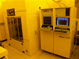
Nikon
NSR-1505G4
The Nikon NSR-1505G4 is a wafer stepper for photolithography. The Nikon NSR-1505G4 uses g-line UV light with a 5x reduction. The Nikon NSR-1505G4 provides better than 750 nm resolution and better than 150 nm alignment.[1][2]
Wafer size
4"
Node / era
better than 750 nm resolution; better than 150 nm alignment
Optics
5" reticle[1]
What it is
How it works
Where it fits in the process flow
General reference — not yet source-verifiedA wafer stepper belongs in the photolithography portion of a semiconductor process flow.
The Nikon NSR-1505G4 is used to transfer patterned features onto wafers after resist coating and before later pattern-transfer steps such as etching or lift-off.
Applications
- Photolithography
What do the numbers mean?
Wafer handling3
Optics & imaging6
Configuration & options2
Where are the manuals?
Generated from public-source data on file. Enter your email to access — nothing is published; details are routed privately.
Not publicly documented
Field notes
No research found yet — worked with this tool? Share what you know.
Frequently asked questions
Not publicly documented
The following facts about the NSR-1505G4 are absent from this record as of this revision. First-hand knowledge or a citation closes a gap; every submission is reviewed before publication.
No publicly documented production dates or lifecycle milestones (introduction, end of production, EOL) for the NSR-1505G4 are on record.
Answerable by: OEM historical records or a trade-press announcement
No publicly documented variants, configuration options, or revision breakpoints of the NSR-1505G4 are on record.
Answerable by: an OEM product catalog or an engineer who ordered or specified the tool
The control-system platform and OS era of the NSR-1505G4 are not on record.
Answerable by: an engineer who operated it or OEM installation records
No publicly documented failure modes or field errata for the NSR-1505G4 are on record.
Answerable by: a field service engineer, process engineer, or maintenance technician
No publicly documented compatible parts, consumables, or accessories for the NSR-1505G4 are on record.
Answerable by: an OEM parts catalog or a service engineer
No research found yet — worked with this tool? Share what you know.
Sources & citations
Sources (4)Every fact above is drawn from these public sources
- [1]nanofab.ece.cmu.edu — nanofab.ece.cmu.edunanofab.ece.cmu.edu
- [2]NSR-1505G4 — Nikon | Specs, Sourcing & Service | Waferpedia — waferpedia.comwaferpedia.com
- [3]Nikon NSR-1505G4 family | Waferpedia — waferpedia.comwaferpedia.com
- [4]Equipment - Claire & John Bertucci Nanotechnology Laboratory - College of Engineering - Carnegie Mellon University — nanofab.ece.cmu.edunanofab.ece.cmu.edu
Last updated Oct 7, 2026.
Compare with similar tools
View all →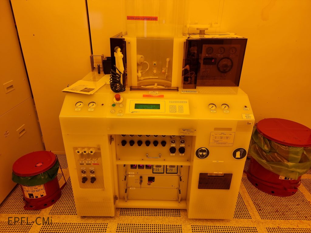
The Hamatech HMR900 is a mask processor for Cr-plate wet processing or cleaning.

The Nanoscribe Photonic Professional GT+ is a 3D nanoprinter for two-photon polymerization using an infrared 780 nm femtosecond laser.
Brooks 017-0146-01 is a prealigner manufactured by Brooks.