ASML
5500/80
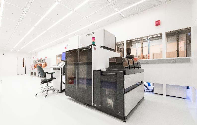
The ASML 5500/80 is an i-line wafer stepper. The ASML 5500/80 is set up for 4-inch wafers. The ASML 5500/80 is convertible to 3-inch or 6-inch platforms.[1][2]
Wafer size
4-inch wafers; convertible to 3-inch or 6-inch platforms
Node / era
500nm resolution
Performance
<70nm[1]
Optics
500nm[1]
What it is
General reference — not yet source-verifiedThe ASML 5500/80 is an i-line wafer stepper used for photolithography on wafers.
How it works
General reference — not yet source-verifiedA wafer stepper projects a patterned image from a mask onto photoresist-coated wafers through a reduction optical system. The tool exposes one field at a time and then advances the wafer to the next field for repeated pattern transfer.
Where it fits in the process flow
General reference — not yet source-verifiedThe ASML 5500/80 sits in the photolithography portion of wafer fabrication. The tool is used after resist coating and alignment and before the developed pattern is transferred into underlying films by later process steps.
What do the numbers mean?
Wafer handling2
Optics & imaging1
Performance1
Dimensions & facilities1
Configuration & options4
Where are the manuals?
Generated from public-source data on file. Enter your email to access — nothing is published; details are routed privately.
Not publicly documented
Field notes
No research found yet — worked with this tool? Share what you know.
Frequently asked questions
Not publicly documented
The following facts about the 5500/80 are absent from this record as of this revision. First-hand knowledge or a citation closes a gap; every submission is reviewed before publication.
No publicly documented production dates or lifecycle milestones (introduction, end of production, EOL) for the 5500/80 are on record.
Answerable by: OEM historical records or a trade-press announcement
No publicly documented variants, configuration options, or revision breakpoints of the 5500/80 are on record.
Answerable by: an OEM product catalog or an engineer who ordered or specified the tool
The control-system platform and OS era of the 5500/80 are not on record.
Answerable by: an engineer who operated it or OEM installation records
No publicly documented failure modes or field errata for the 5500/80 are on record.
Answerable by: a field service engineer, process engineer, or maintenance technician
No publicly documented compatible parts, consumables, or accessories for the 5500/80 are on record.
Answerable by: an OEM parts catalog or a service engineer
No research found yet — worked with this tool? Share what you know.
Sources & citations
Sources (4)Every fact above is drawn from these public sources
- [1]nanofab.ece.cmu.edu — nanofab.ece.cmu.edunanofab.ece.cmu.edu
- [2]waferpedia.com — waferpedia.comwaferpedia.com
- [3]waferpedia.com — waferpedia.comwaferpedia.com
- [4]Equipment - Claire & John Bertucci Nanotechnology Laboratory - College of Engineering - Carnegie Mellon University — nanofab.ece.cmu.edunanofab.ece.cmu.edu
Last updated Oct 5, 2026.
Compare with similar tools
View all →Brooks 017-0146-01 is a prealigner manufactured by Brooks.
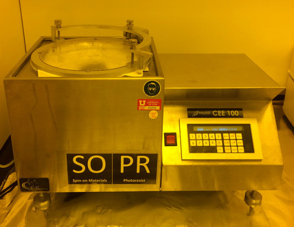
The CEE 100 is a lithography spin coater/developer tool that accepts up to 6-inch wafers and supports programmable multi-step processing.