Tokyo Electron
CleanTrack ACT 8
The Clean Track ACT 8 is an industry-standard wafer coater and developer. The Clean Track ACT 8 supports DUV lithography with an in-line exposure unit interface. The Clean Track ACT 8 is configured for 100 mm (4") wafers.[1]
Wafer size
100mm
Node / era
DUV lithography
Vacuum
4 for photoresist (COT), 2 for BARC (BCT)[1]
Performance
High throughput in a small footprint[1]
Gas delivery
TMA238WA[1]
How it works
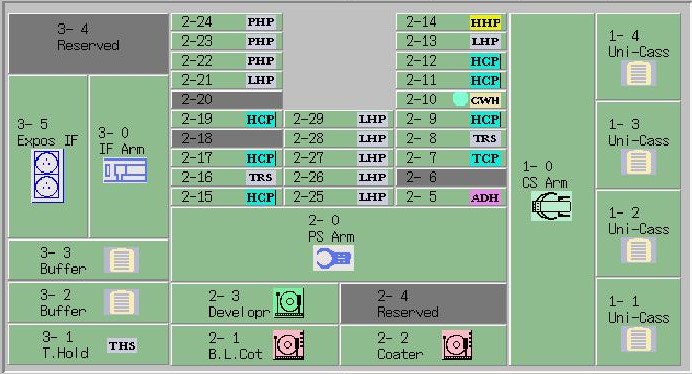
The ACT8 is composed of three main blocks: the Carrier Station Block (CSB), the Process Block (PRB), and the Interface Block (IFB). The CSB is the interface with the external world and features four cassette ports for wafer cassettes. The PRB is the tool processing core, featuring spinning units such as coaters and developers, as well as thermal plates. The Interface Block allows wafers to pass to the next block.[1]
Spinning units in the PRB include the Bottom-layer Coater for bottom antireflective coating, the Coater for photoresist spin, and the Developer for photoresist development. Inside spinning units, environmental conditions are tightly controlled with laminar flow of air at regulated temperature, humidity, and air velocity. Thermal plates come in different types: low-temperature hot plates for non-critical bakes, high-temperature hot plates for curing or hardening, high-speed chill plates for fast cooldown, and adhesion promoter plates for vapor-phase HMDS treatment. Precision hot plates feature integrated cooling arms and advanced heating zones for post-exposure bake control.[1]
The track includes a Carrier Robot Arm that shuttles wafers between cassettes and the Process Block. A Process Robot Arm transports wafers between modules using up to three pincettes that perform fast wafer exchanges. An automatic maintenance routine uses a wash disc to clean the cup and splash ring in the coating and developing units. The track is typically configured to operate in-line with a separate exposure tool, forming a lithography cluster.[1]
Where it fits in the process flow
In a semiconductor fabrication line, the ACT8 track sits upstream of the exposure step, performing resist coating and baking before exposure and development after exposure. The track is configured to operate in-line with a separate stepper, forming a complete lithography cluster. The cluster processes wafers through the coater, exposure tool, and developer without breaking vacuum or exposing wafers to ambient contamination.[1]
Applications
The ACT8 track supports DUV lithography processes. The track is used for applying bottom antireflective coatings, photoresist, and for developing resist patterns. Thermal processing includes dehydration, post-apply bake, post-exposure bake, and hard bake steps.[1]
- DUV lithography
- Photoresist coating
- Photoresist development
- Anti-reflective coating processing
- Post-exposure bake and related thermal processing
Why won't it start?
Documented failure modes, common issues, and field considerations.
- Wafers going through the track must have a clean backside.
- Small particles can hinder printing of small features and/or contaminate the wafer stage for subsequent batches.
- Wafers with contaminated or dirty backsides should be removed from the batch.
- Wafer stage cleaning is described as delicate, complex, wearing, time-consuming, and requiring recalibration.
- Users liable of wafer stage contamination will be billed cleaning hours and may lose access to the machine.
- The source warns that using the wrong cassette type may put the carrier robot arm and wafers in serious danger.
What do the numbers mean?
Vacuum & pumping2
Wafer handling16
- Wafer size
- Interface Unit (IRA) for Canon FPA-3000 i5 stepper including one multi-buffer unit and Wafer edge exposure (WEE)[2]
Gas & chemistry11
Optics & imaging3
Performance3
- Thermal Plates
- Low-temperature Hot Plate, High-temperature Hot Plate, High-speed Chill Plate, ADHesion plates, Precision Hot Plates, Transition Station, Transition Chill Plate[1]
Control & software5
- Temperature/humidity control
- Internal laminar flow with regulated temperature, humidity, and cup temperature/humidity controller (T&H)[1]
Configuration & options12
- In-line with ASML PAS5500/350C stepper forming a DUV lithography cluster[1]
What does it need to run?
Site utility requirements, footprint, and infrastructure needed to install and operate this tool. Sourced from public records.
- Cluster configurationCoater and developer track in-line with an ASML PAS5500/350C stepper[1]
- Process materialsKrF photoresist and ancillary anti-reflective coatings[1]
- Resist pump lines4 for photoresist (COT), 2 for BARC (BCT)[1]
- Developer lines2 pressure-driven lines[1]
- Developer usedTMA238WA[1]
- Solvent usedMicroposit EC Solvent (Dupont)[1]
- Spinning UnitsBottom-layer Coater (BCT), Coater (COT), Developer (DEV)[1]
- PhotoresistKrF photoresist (M108Y, M35G)[1]
- DeveloperTMA238WA[1]
- External ModulesAC Power Box, Chemical Cabinet, Temperature and Humidity Controller, Thermostatic Water Supply[1]
- Photoresist typesM108Y (JSR Corporation) and M35G[1]
- Chemical filtersULPA chemical filters[1]
- Photoresist chemistryKrF photoresist[1]
Where are the manuals?
Generated from public-source data on file. Enter your email to access — nothing is published; details are routed privately.
Not publicly documented
Field notes
No research found yet — worked with this tool? Share what you know.
Frequently asked questions
What are the three main blocks of the ACT 8?
The machine is composed of a Carrier Station Block (CSB), a Process Block (PRB), and an Interface Block (IFB).[1]
What spinning units are found in the Process Block?
The Process Block contains a bottom-layer coater (BCT) for antireflective coatings, a coater (COT) for photoresist, and a developer (DEV).[1]
What thermal plates are available in the ACT 8?
The machine includes low-temperature hot plates (LHP), high-temperature hot plates (HHP), high-speed chill plates (HCP), precision hot plates (PHP), and an adhesion promoter plate (ADH) for HMDS vapor treatment.[1]
Not publicly documented
The following facts about the CleanTrack ACT 8 are absent from this record as of this revision. First-hand knowledge or a citation closes a gap; every submission is reviewed before publication.
No publicly documented production dates or lifecycle milestones (introduction, end of production, EOL) for the CleanTrack ACT 8 are on record.
Answerable by: OEM historical records or a trade-press announcement
No publicly documented variants, configuration options, or revision breakpoints of the CleanTrack ACT 8 are on record.
Answerable by: an OEM product catalog or an engineer who ordered or specified the tool
The control-system platform and OS era of the CleanTrack ACT 8 are not on record.
Answerable by: an engineer who operated it or OEM installation records
No publicly documented compatible parts, consumables, or accessories for the CleanTrack ACT 8 are on record.
Answerable by: an OEM parts catalog or a service engineer
No publicly hosted manuals, SOPs, or datasheets for the CleanTrack ACT 8 are on record.
Answerable by: university cleanroom staff or an OEM application specialist
Sources & citations
Sources (5)Every fact above is drawn from these public sources
- [1]epfl.ch — epfl.chepfl.ch
- [2]Inventory photo
- [3]Inventory photo
- [4]Inventory photo
- [5]Inventory photo
Last updated Oct 8, 2026.
Compare with similar tools
View all →ASML PAS 5500/300 is a deep-UV stepper photolithography tool configured for 4-inch wafers.

The GCA 6100 C Wafer Stepper is a lithography tool for 100 mm wafers with a 150 mm X/Y stage travel and an AWH1 automatic wafer handler.
The OAI 808 Aligner is a semi-automated, four-camera, optical front- and backside mask aligner with stated alignment accuracy of 1µm to 2µm.
The OAI Model 800 Mask Aligner is a semi-automated, four-camera, optical front- and backside mask aligner with motorized backside focus, motorized auto leveling, and auto gap setting.
