JEOL
JSM-7500F
The JEOL 7500F HRSEM provides ultrahigh resolution of 0.8 nm at 30 kV and 1 nm at 1 kV, useful for soft-matter studies.[1]
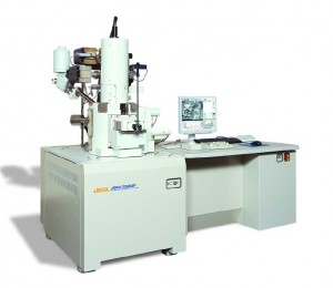
What it is
General reference — not yet source-verifiedA scanning electron microscope forms high-magnification images by scanning a focused electron beam across a specimen and detecting signals generated from the surface region.
How it works
General reference — not yet source-verifiedA field emission SEM is used to obtain detailed surface information, and the instrument class is commonly used with analytical attachments for elemental and structural examination.
Where it fits in the process flow
General reference — not yet source-verifiedA scanning electron microscope sits in the inspection and characterization portion of a fabrication flow rather than in core material deposition or pattern transfer steps.
What can it run?
Process applications and technology nodes documented for this tool.
- High-resolution imaging
- Conventional imaging
- Study of a wide range of solid materials
- Soft-matter studies
- Imaging of soft or insulating samples
- Chemical characterization via spectra or element maps
What do the numbers mean?
Power & electrical1
Gas & chemistry1
- Chemical characterization
- EDAX Energy Dispersive x-ray spectrometer (EDS) available for spectra or element maps[1]
Optics & imaging9
- Detectors
- Secondary electron, backscattered electron, and scanning-transmission electron detectors[1]
- Gentle beam mode
- Stage biasing system reduces electron beam energy for imaging soft or insulating samples without coating[1]
- Detectors
- Secondary and backscattered electron detectors, scanning-transmission electron detector[1]
- Application
- high-resolution imaging of large specimens; suitable for observing shallow surfaces of samples[2]
Configuration & options9
- Unique Feature
- Gentle Beam (GB mode) for top-surface imaging with ultra-low energy incident electrons[3]
What does it need to run?
Site utility requirements, footprint, and infrastructure needed to install and operate this tool. Sourced from public records.
Where are the manuals?
Generated from public-source data on file. Enter your email to access — nothing is published; details are routed privately.
Not publicly documented
Field notes
No research found yet — worked with this tool? Share what you know.
Frequently asked questions
What are the primary components of an instrument in this class?General reference — not yet source-verified
The core components include an electron gun, a column of electromagnetic focusing and scanning lenses, a sample stage, a vacuum system, secondary and backscattered electron detectors, and a computer interface for operations and image analysis.
What sample preparation is typically required for this class of machine?General reference — not yet source-verified
Samples must be compatible with high vacuum. Non-conductive samples often require a thin conductive coating, such as gold or carbon, applied to prevent charging under the electron beam and to improve image quality.
How is measurement accuracy ensured in metrology applications?General reference — not yet source-verified
Accuracy is maintained through routine calibration using traceable reference standards, correction of image distortions, and strict control of the operating environment to minimize drift and vibration during measurement.
Not publicly documented
The following facts about the JSM-7500F are absent from this record as of this revision. First-hand knowledge or a citation closes a gap; every submission is reviewed before publication.
No publicly documented production dates or lifecycle milestones (introduction, end of production, EOL) for the JSM-7500F are on record.
Answerable by: OEM historical records or a trade-press announcement
No publicly documented variants, configuration options, or revision breakpoints of the JSM-7500F are on record.
Answerable by: an OEM product catalog or an engineer who ordered or specified the tool
The control-system platform and OS era of the JSM-7500F are not on record.
Answerable by: an engineer who operated it or OEM installation records
No publicly documented failure modes or field errata for the JSM-7500F are on record.
Answerable by: a field service engineer, process engineer, or maintenance technician
The process node or technology generation of the JSM-7500F is not on record.
Answerable by: an OEM datasheet or a fab qualification report
No research found yet — worked with this tool? Share what you know.
Sources & citations
Sources (3)Every fact above is drawn from these public sources
- [1]nano.upenn.edu — nano.upenn.edunano.upenn.edu
- [2]web.archive.org — jeol.co.jp (Mar 19, 2017)web.archive.org
- [3]jeol.comjeol.com
Last updated Oct 3, 2026.
Compare with similar tools
View all →The KLA .204 PSL Wafer is an 8-inch NIST-traceable reference wafer compatible with Surfscan 6xy0 and Sp1 particle counters.
KLA .496 PSL Wafer is an 8-inch NIST traceable wafer stated to be capable on Surfscan 6xy0 and SP1.
The KLA .498 PSL Wafer is a NIST traceable reference wafer.
