GCA
6300 DSW
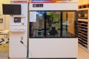
The GCA 6300 DSW is a step-and-repeat photolithography wafer stepper. The GCA 6300 DSW uses a 5:1 reduction lens and can be configured with either a g-line (436 nm) or i-line (365 nm) exposure wavelength.[1][2]
What it is
General reference — not yet source-verifiedThe GCA 6300 DSW is a wafer stepper designed for projection photolithography in semiconductor fabrication. Like all wafer steppers, it uses a reduction lens to project the image of a mask (reticle) onto a resist-coated substrate, then steps the substrate to expose multiple fields in a step-and-repeat pattern. The DSW designation stands for Direct Step on Wafer, indicating that the machine exposes each die or field individually by moving the wafer under a stationary lens.
What can it run?
Process applications and technology nodes documented for this tool.
- photolithography
- step and repeat exposure
- high-resolution lithography
- critical alignment
What do the numbers mean?
Wafer handling10
Optics & imaging22
Performance3
Dimensions & facilities1
Configuration & options13
Vintage & configurations
Documented models & variants
Where are the manuals?
Publicly hosted documents referencing this tool, linked at their original location. Hosted by the linked institutions — availability may change.
- GCA 5X Operation ManualManualcornell.edu
- GCA 5X Resist InformationDocumentcornell.edu
Generated from public-source data on file. Enter your email to access — nothing is published; details are routed privately.
Not publicly documented
Field notes
No research found yet — worked with this tool? Share what you know.
Frequently asked questions
What does DSW stand for?General reference — not yet source-verified
DSW stands for direct step on wafer, describing the stepper's method of exposing one field at a time and then stepping the wafer to the next exposure position.
How does a wafer stepper differ from a full-wafer aligner?General reference — not yet source-verified
A wafer stepper exposes and aligns one field at a time through a lens, then steps the wafer to the next position. A full-wafer aligner exposes the entire wafer in a single exposure.
What factors influence overlay and image quality on a stepper?General reference — not yet source-verified
Overlay quality depends on wafer-stage accuracy, alignment-mark quality, and thermal stability. Image quality depends on focus, illumination uniformity, and projection-lens performance.
What routine maintenance is typical for this class of equipment?General reference — not yet source-verified
Routine maintenance includes cleaning optical surfaces, monitoring exposure-source performance, verifying stage calibration, and checking the alignment system.
Not publicly documented
The following facts about the 6300 DSW are absent from this record as of this revision. First-hand knowledge or a citation closes a gap; every submission is reviewed before publication.
No publicly documented production dates or lifecycle milestones (introduction, end of production, EOL) for the 6300 DSW are on record.
Answerable by: OEM historical records or a trade-press announcement
The control-system platform and OS era of the 6300 DSW are not on record.
Answerable by: an engineer who operated it or OEM installation records
No publicly documented failure modes or field errata for the 6300 DSW are on record.
Answerable by: a field service engineer, process engineer, or maintenance technician
No publicly documented compatible parts, consumables, or accessories for the 6300 DSW are on record.
Answerable by: an OEM parts catalog or a service engineer
The operating principle of the 6300 DSW is not documented in this record.
Answerable by: an equipment physicist or OEM application engineer
No research found yet — worked with this tool? Share what you know.
Sources & citations
Sources (2)Every fact above is drawn from these public sources
- [1]cnfusers.cornell.edu — cnfusers.cornell.educnfusers.cornell.edu
- [2]wiki.nanofab.ucsb.edu — wiki.nanofab.ucsb.eduwiki.nanofab.ucsb.edu
Last updated Oct 9, 2026.
Compare with similar tools
View all →
The MA / BA Gen4 Pro Series is a semi-automated mask aligner and bond aligner system supporting wafers up to 150 mm / 200 mm, with capabilities for exposure, UV bonding, fusion bonding, micro- and nanoimprinting, and selective plasma activation.
The MA100 / 150e Gen2 is an automated mask aligner for proximity exposure, supporting wafer sizes up to 150 mm.

The Karl Suss MA6 is a high-resolution semi-automated photolithography mask aligner for research, development, and small-volume production.
